+91-880-055-7974 | newton@nippondata.com

Electronic Design and Automation

Home / EDA

EDA

Electronic Design and Automation – EDA Services

Electronic Design Automation, or EDA, is a market segment consisting of software, hardware, and services with the collective goal of assisting in the definition, planning, design, implementation, verification, and subsequent manufacturing of semiconductor devices, or chips. Regarding the manufacturing of these devices, the primary providers of this service are semiconductor foundries, or fabs. These highly complex and costly facilities are either owned and operated by large, vertically integrated semiconductor companies or operated as independent, “pure-play” manufacturing service providers. This latter category has become the dominate business model.

Electronic Design and Automation

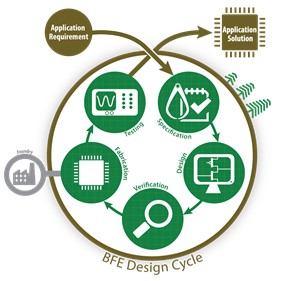
Nippon (EDA Division) is an advanced technology services provider offering comprehensive solutions from concept to prototype, in the semiconductor space. We offer an integrated portfolio of services to our clients in key domains including digital, analog, high speed physical interface IP, Embedded Memory Compiler and SoC Modelling.

We are the preferred semiconductor design service partners to several companies in Automotive, Consumer Electronics, Industrial IoT and Medical electronics space. We help our customers achieve their time-to-market window by delivering first pass silicon designs and engage with product engineering teams across the globe to design System-on-Chip. Nippon has centers in USA, UK, India, Africa, Middle East, Thailand and Canada.

      GET EXPERT CONSULTATION

      leave your contact details and our experts will call you back

    • Enter your Name

    • Enter your Email

    • Enter your Mobile

    • Enter your Message

    Major areas of this business

    • Architecture Analysis
    • Good Design
    • Verification
    • Netlist Release
    • Physical Design
    • Foundry Services & Manufacturing
    • Validation
    • Application Software Development

    EDA Design Flow

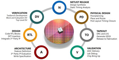
    The EDA design flow can be divided into two designs, digital design and analog design. In digital design a circuit is described using a hardware description language, followed by simulation of circuit design, synthesis, place & route and post layout simulation. In analog design, a circuit is captured, followed by simulation, physical design, layout extraction and post layout simulation. The combined layouts of digital and analog designs are used in a manufacturing facility to produce an electronic chip.

    EDA Design Cycle

    1. Analog Design & Layout Std. Cells, Memories and IOs

    ANALOG & MIXED SIGNAL ENGINEERING

    Our team has in-depth expertise on variety of IPs such as SerDes (10, 16, 30 & 56 Gbps), DDRphy, USB 2.0, MIPIphy and Power management. We have also handled expanded portfolios of Data converters, clock circuits such as PLL, DLL & oscillators, Regulators, Bias, Bandgap references, Temperature sensors, UVLOs etc. in almost all leading foundries at technologies varying from 500nm BCD to 7nm Finfet. Multiple full chip and IP level tape out has been successfully done with first pass silicon.

    What sets us unique is that the knowledge gained is shared among other team members across sites to close the skill gap at any experience level.

    STANDARD CELL SOLUTIONS

    In the past, our team has delivered multiple std cell libraries at 90nm, 65nm, 45nm, 32nm, 28nm, 20nm, 16FF, 14nm, 10nm etc. with leading foundries. These libraries include High performance, High density, 11T, 9T, 7.5T, 6T design. We are also expert when it comes to migration of libraries to latest technologies.

    IO SOLUTIONS

    Our team has delivered IO layout from 250nm to 16nm technologies. These includes GPIOs, LVCMOS, LVTTL, LVDS, DDR etc. with Analog/Power ring. ESD requirements for HBM, MM, CDM were taken care.

    2. FPGA Design, Emulation and Post-Silicon Validation

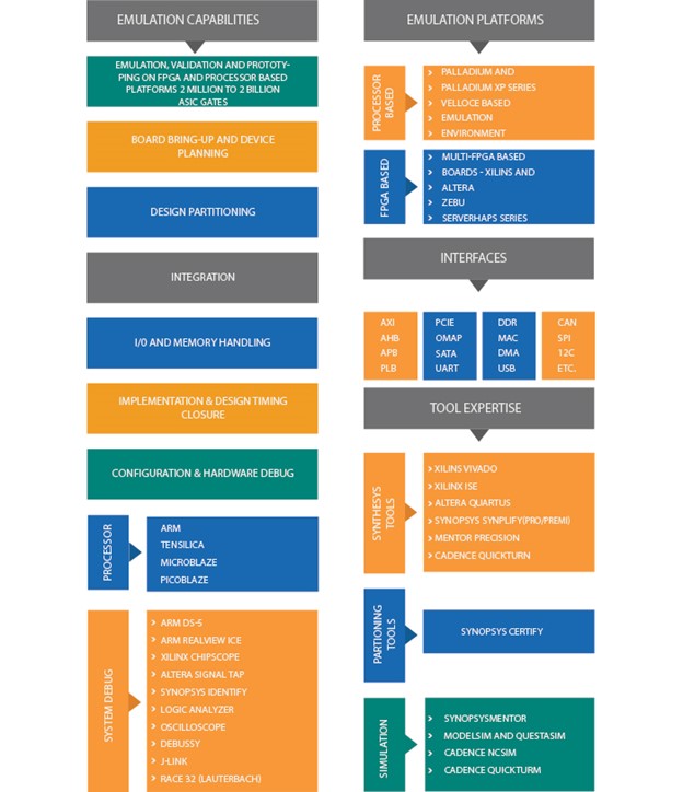
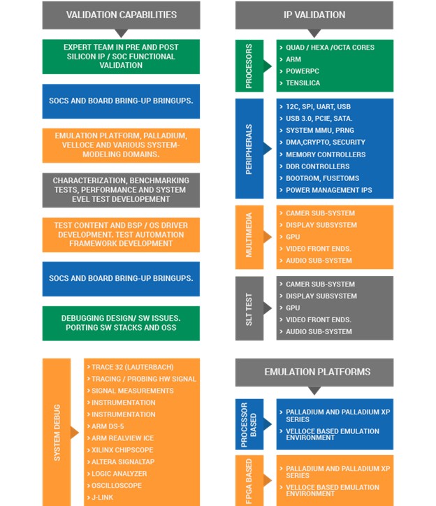
    Expertise in Prototyping and Emulation of complex IC designs for faster system debug and software bring-up. The team has lots of experience in the area of board bring-up, development of test automation frameworks, error diagnosis and system debug, OS driver development, debugging software stacks, characterization and benchmarking tests.

    POST SILICON VALIDATION

    The Post Silicon Validation(PSV) team at Nippon is a large group of technically strong engineers in the areas mentioned below. The team is well-led, closely-knit, and has received very good feedback from the industry. Further, Nippon has got lab facilities and training sessions exclusively for PSV engineers.

    Post Silicon Validation

    FPGA DESIGN & EMULATION

    Nippon’s team in Emulation and FPGA design have hands-on experience doing the following activities at several of our clients:

    FPGA DESIGN & EMULATION

    We have over 15 years of experience in providing end-to-end semiconductor services leveraging cutting edge technology solutions.

    Design Services

    Our team of experts has experience on various aspects of RTL Design flow on chips that are extensively used in networking, mobile, automotive, multimedia and processor sectors.
    Our design service suite consists of the following
    • SoC Architecture
    • IP Micro Architecture
    • RTL (Register-Transfer Level) Design
    • SoC Integration
    • Linting, CDC
    • Low Power Checks
    • Synthesis
    • LEC (Logical Equivalence Check)
    • Timing & DFT

    ASIC Verification

    Digital’s skilled verification team has proven – expertise in comprehensive verification services helping deliver bug free chip.
    Our verification service consists of the following
    Experience bug free software with —– Digital’s test automation frameworks and error diagnosis system. Our team of competent engineers working in the FPGA Emulation and Validation team are experts in prototyping and emulating complex IC designs for streamlined system debugging and software bring-up. Be it board bring-up, development of test automation frameworks, error diagnosis or system debug, our FPGA Emulation and Validation Services team can provide you with the most suitable solution.
    Our distinguished team has experience in working with various semiconductor industries across the globe for System Level Testing, Signal Integrity, Bench Marking, Test Content Development and Automation.

    ASIC Verification

    • GLS
    • FPGA design
    • FPGA prototyping
    • Emulation
    • Post Silicon Validation
    • IP Validation
    • Protocol Qualification
    • Processor Based Emulation
    • Digital has over a decade of experience in providing hardware and software design, development and testing services for Automotive, Industrial Control and solutions around IoT technology. Our technical team has experience in complete software development lifecycle, with involvement right from requirements analysis stage up to the final release and acceptance of the software.
    • With experience in various hardware platforms and processor architectures as well as real time OS platforms, —– Digital can enable embedded system development involving hardware design, software development and hardware/software integration. With our partner-ecosystem, we can enable functional prototyping, pre-compliance testing and volume manufacturing.

    He architecture consists of the following components

    System Software
    Operating Software
    Application
    Platforms
    Middleware – Multimedia
    Middleware – Connectivity
    • KEYWORDS
    • Eda
    • Staffing
    • Professional services
    • IT consulting
    • Manpower
    • Semiconductor